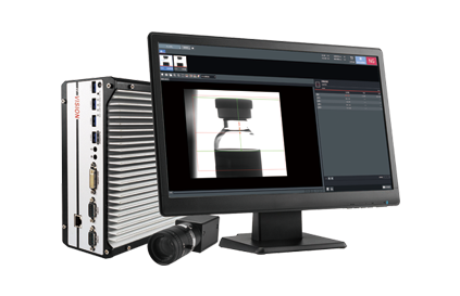
One-stop-solution for machine vision products.
Mstar Technologies, Inc, as a leading provider of a comprehensive Machine Vision System in China, was founded in March 2012, located in Zhejiangoverseas High-Level Talents Innovation Park. Mstar Technologies, Inc, is a company engaged in the area of development and production of machine vision products including machine vision system, industrial camera, FA lenses, machine vision lightings, infrared thermal cameras and etc..
Ask our Engineers about your application!Do you have an important technical question?Are you looking for the solution for your application?
PCB Defect Detection

PCB Defect Detection
About hundreds of inspection points on PCB are coated with solder paste. In order to ensure the product quality, it is necessary to detect the defects of solder paste on PCB, that is, to detect the coverage area of solder paste.
Background
Requirement Description:
1. The original method of area array camera and two-dimensional motion manipulator was used to shoot. The copper plate was static while the camera was moving. The naked eye detection could not save the image. Therefore, the scheme needs to add the functions of automatic identification, data statistics and image storage.
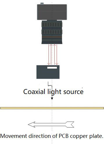
2. The copper plate has a mechanical structure to drive intermittent horizontal movement along the length direction; when the area array camera is finished, the copper plate is transported to the next station, so a linear array camera can be set up between the two stations for shooting, and the copper plate passes through the bottom uniformly.
3. Pictures need to be stored for two years, and large space hard disk is needed to store the images without compression. Therefore, it is necessary to add image compression function, output JPG format pictures, and establish index according to production batch number to facilitate searching.
Technical Requirements:
1. The size of the copper plate is about 260 * 80mm, and there are about 400 detection points on it, which are coated with solder paste.
2. The size of solder paste is about 1 mm * 1 mm, and the coverage area of solder paste needs to be tested.
Structure
PCB defective product detection system uses linear array camera, KF series industrial lens and coaxial light source to build a vision system, which is installed on the production line. PCB board passes through the image acquisition at a constant speed below. After the collected image is sent to the visual processor, the algorithm tool of the vision system platform can detect whether there are defects in each solder paste point and the number of defects in all solder paste points.
Advantages
1. Accurate identification: accurately identify the area, X-axis offset and y-axis offset of solder paste points.
2. Statistical analysis: count the bad distribution of different defined areas on PCB, and improve the process pertinently.
3. Fast and efficient: the moving speed of copper plate is 1m / s, and the dwell time on each station is 10s. Preliminary calculation shows that the camera works at 25K line frequency, and image processing can be completed in 10s.
4. Complete functions: add functions of automatic identification, data statistics and picture storage.


Mstar Technologies, Inc, as a leading provider of a comprehensive Machine Vision System in China, was founded in March 2012, located in Zhejiangoverseas High-Level Talents Innovation Park. Mstar Technologies, Inc, is a company engaged in the area of development and production of machine vision products including machine vision system, industrial camera, FA lenses, machine vision lightings, infrared thermal cameras and etc..